Hardware notes
Schematic
Designed with KiCad.
You can view the schematic and PCB layout in your browser: view KiCad files in kicanvas.org.
PCB
Specifications
- 4 layers
- FR-4
- 1 mm thickness
- 1 oz copper on all layers (including internal)
The design around the BQ25792 with its inductor and capacitors follows the guidelines given in the datasheet, and takes the EVM design as a basis. However, due to space constraints and the oblong shape, some compromises in the PCB layout had to be made: the BQ25792 has been rotated 180° relative to the reference design, making the switching nodes slightly longer and closer to other traces. Care was taken to keep them isolated from other traces by intermediate ground plane layers.
JLCPCB order settings
When ordering from JLCPCB, the files located in pcb/jlcpcb/production_files can be uploaded directly.
- Layers: 4
- Dimensions: 69 x 19 mm (will be increased automatically for edge rails)
- PCB Thickness: 1.0 mm
- Material: FR4
- Surface Finish: LeadFree HASL or ENIG
- Outer Copper Weight: 1 oz
- Inner Copper Weight: 1 oz (!)
- Via Covering: Plugged
- PCBA Type: Standard
- Assembly Side: Both Sides
- Edge Rails/Fiducials: Added by JLCPCB
- Depanel boards & edge rails before delivery: Yes
Side panel
- Aluminum 6061
- Bead-blasted, hardcoat-anodized, and silkscreened
Kit components
A full KXUSBC2 "kit" requires the following components:
- KXUSBC2 PCB, assembled on both sides
- Custom side panel
- 3 x Receptacle (unless assembled by PCB factory)
- TE Connectivity 2307725-3
- DigiKey 17-2307725-3CT-ND
- 2 x Standoff M2.5 3 mm height (unless assembled by PCB factory)
- Würth Electronics 9774030151R
- DigiKey 732-7083-1-ND
- Thermal pad 10x6 mm, 4 mm height
- Stranded silicone insulated wires, AWG 22, red/white 60 mm ea.
- 2 x Solder pin
- Mill-Max 3132-0-00-15-00-00-08-0
- DigiKey ED90540-ND
- 2 x Solder receptacle
- Mill-Max 8827-0-15-15-16-27-04-0
- DigiKey ED1304-ND
- Heat shrink tube 2.5 x 15 mm
- Thermistor (optional)
- NTC 10k
- DigiKey 2259-RH18-6Y103FB-075-S-ND
Cost
Most of the parts are relatively low cost, and the board was designed so that it can be produced and assembled by low-cost services like JLCPCB, with almost all passive components from the “Basic” component selection, which doesn't incur component-loading fees. Most components are on the top side, but due to space constraints, some had to be placed on the bottom side as well. Traces, via holes etc. are fairly large to avoid precision PCB costs.
Bill of materials
The total BOM at qty. 10 is around $30/pc. (including PCB production and assembly of both sides), plus $12/pc. for the CNC milled, anodized and silkscreen printed side panel.
Efficiency
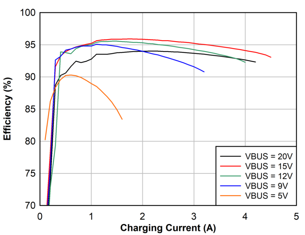
The graph above is taken from the BQ25792's datasheet. I've done some casual measurements, both using the BQ25792's internal ADC and shunts, and with external power meters, and they agree with the data in the graph: around 95% when charging from 15 V input, and between 85% and 90% from 5 V (depending on the current). There seems to be no problem dissipating the maximum possible loss of around 3 W through the side panel (thermal pad placed between the IC and the panel), and in any case, the charger IC has thermal regulation and shutdown.
Power connection to the KX2
Like the KXIBC2, the KXUSBC2 is intended to be wired to the “E” and “B” pads on the KX2 RF PCB (under the battery) for connection to the external DC jack and the internal battery jack, respectively. Refer to the KXIBC2 manual for details.
- Wire lengths, measured from the pad on the KXUSBC2 to the tip of the connector pin attached to the wire: E 28 mm, B 40 mm.
- Receptacle pins for soldering to the KX2 PCB, probably also used by Elecraft for factory installation: Mill-Max 8827-0-15-15-16-27-04-0. Mating pin for crimping or soldering to wire: Mill-Max 3132-0-00-15-00-00-08-0 (for 22-24 AWG).
Measured resistances
The PCB trace resistance between the “B” pad on the RF PCB and the central pin on the internal battery connector was measured to be around 5 mΩ (4T/Kelvin measurement). So although the pad/trace was probably not intended for this much current, it should have no problems handling 3 A.
The ground connection is via a single header pin rated for 2 A only. However, the standoffs with which the board is mounted to the side panel are grounded too. The coating/anodizing of the side panel should be stripped on the backside around the mounting holes, and along the bottom part where it meets other metal case parts (like the original side panel). This will provide a low-impedance ground connection through the side panel. Mounted this way, the resistance between the GND pad near the top edge of the backside of the KXUSBC2 PCB and the shaft of the battery DC plug was measured to be around 10 mΩ (4T/Kelvin measurement).
Supported battery types
The charger has been designed for 3S Li-Ion batteries with a charging voltage of 12.6 V and a capacity of around 3000 mAh. The charging/discharging current limits can be changed in the EEPROM if smaller or larger batteries are used. Always use batteries with built-in protection and balancing circuits.
Using 4S LiFePO₄ batteries
It is also possible to use 4S LiFePO₄ batteries. The charging voltage limit needs to be adjusted in the EEPROM. It is recommended to stay a bit below the limit enforced by the battery's protection circuit. Otherwise, when this voltage is reached during charging, the BMS may react by disconnecting the battery, causing the charging voltage to overshoot. This will manifest itself in a fault condition (red blinking LED), as the charger will detect an over voltage event. Usually 14.2 V is a good upper limit (e.g. some EREMIT batteries cut off at 14.2 V or even slightly below that).
RTC
Some people like to use the clock provided by the KXIO2/KXIBC2 options for logging. The RTC chip that Elecraft uses (PCF2123) is obsolete, and the successors use a different register mapping that would require modifications to the KX2 firmware. As the MCU has spare capacity, I opted to use its internal RTC instead, emulating the few SPI commands that the KX2 uses to read/write the time in firmware. The RTC is clocked by a 32.768 kHz crystal, and the microcontroller consumes extremely little power for keeping the clock running.
The firmware automatically applies a temperature compensation, and one can also calibrate the clock using the KX2's "RTC ADJ" menu as usual.
Unlike the KXIO2/KXIBC2, the KXUSBC2 does not include a supercapacitor to keep the clock running during short power outages while swapping the battery. Having the KXUSBC2 installed means that most people probably won't need to swap out the battery anymore.
The KX2 uses an SPI frequency of 1 MHz (mode 0), and the delay between asserting RTC_CS (active high) and the beginning of the SPI transmission is about 10 µs.
Battery monitoring
The KXUSBC2 includes a similar circuit to the one on the KXIBC2 that allows the KX2 to display the actual battery voltage in the menu. It works by dividing down the battery voltage and buffering it with an op-amp before passing it to the microcontroller in the KX2. The “KXIBC2” menu option must be set to “NOR” in the KX2's configuration menu for this to work.
Of course, the KXUSBC2 itself knows all voltages and currents flowing through it precisely, but it has no way to display those values on the KX2's display, as we cannot modify the firmware.
QRM
A charger like this is somewhat akin to a 10 W PA amplifying a 1.5 MHz square wave into a low-pass filter. Having that right inside a sensitive HF rig, and even electrically connected to it, one might expect QRM mayhem. I thought so too, and thus the firmware defaults to automatically suspending charging while the KX2 is on, so one can still use an external power supply to power the KX2 while operating, without any QRM from the charger.
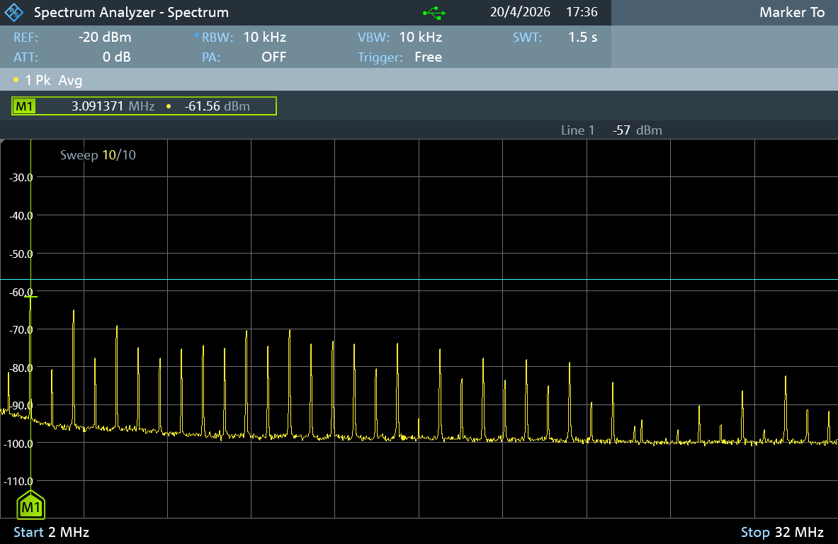
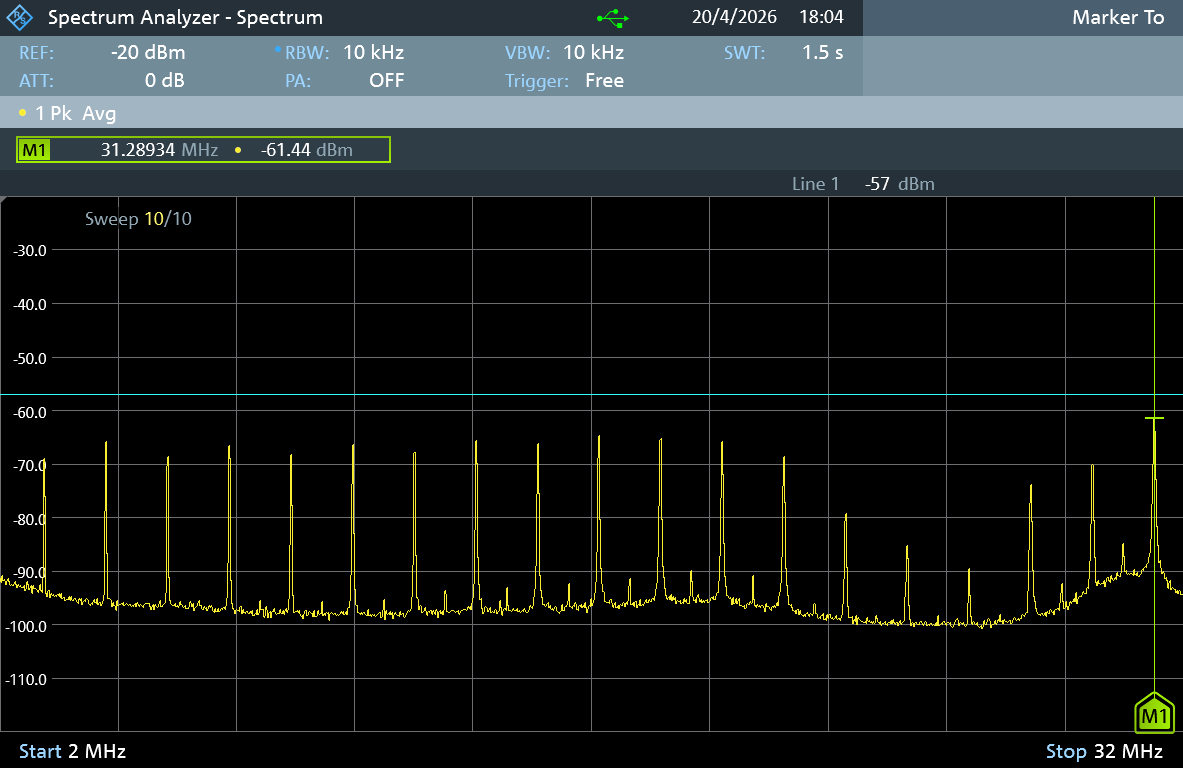
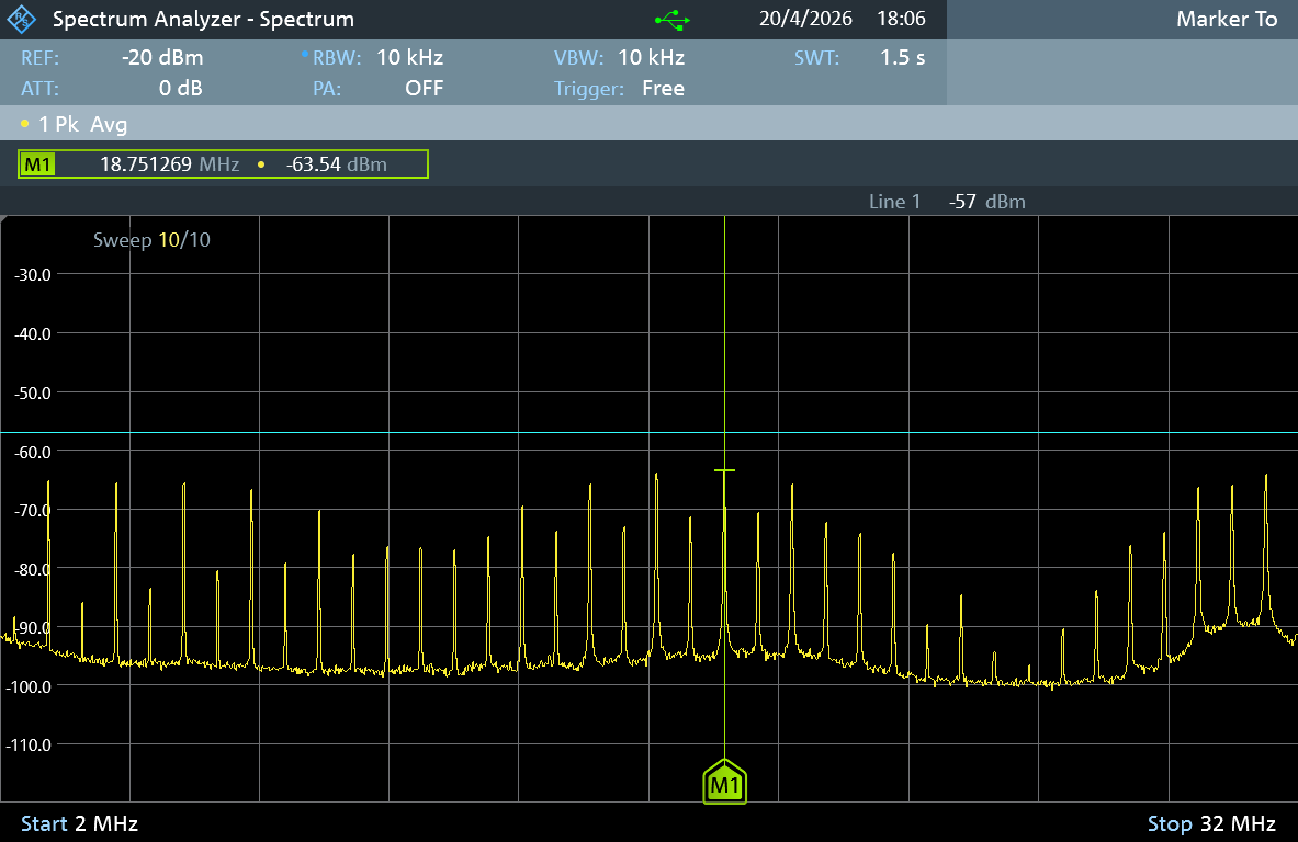
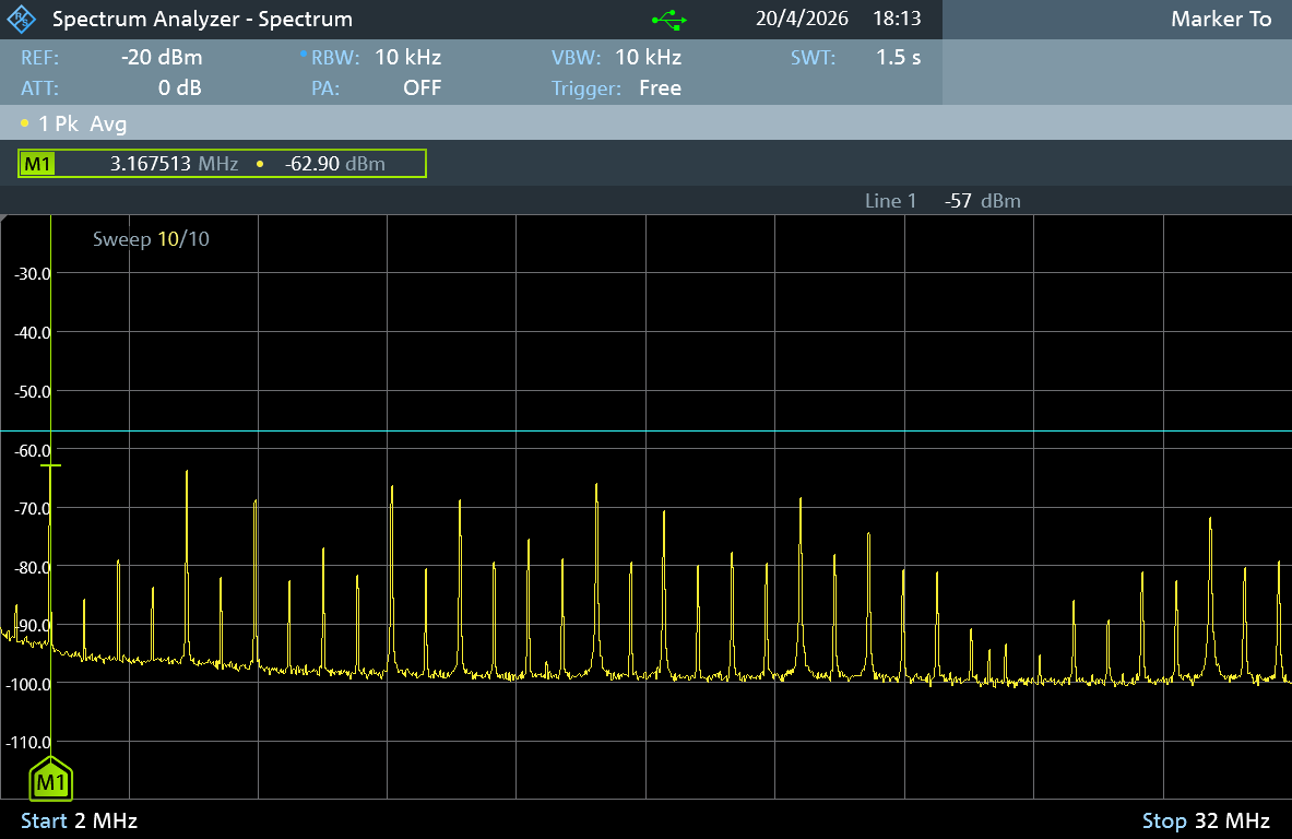
I did some lab testing with a dummy load connected to the KX2. Result: while charging the KX2 at 28 W from a 15 V PD source, I noticed that the noise floor increased from S0 to around S1 on 80-10m (preamp on). The only really strong signal that I could find in amateur bands was the 9th harmonic of the switching frequency, which varied around 9 * 1.55 = 13.95 MHz and 9 * 1.58 = 14.22 MHz in my test (the charger IC uses an RC oscillator), resulting in S7 QRM in a range of about 10 kHz somewhere in the lower half of the 20m band. Results in reverse mode (charging an iPad at 28 W) were similar.
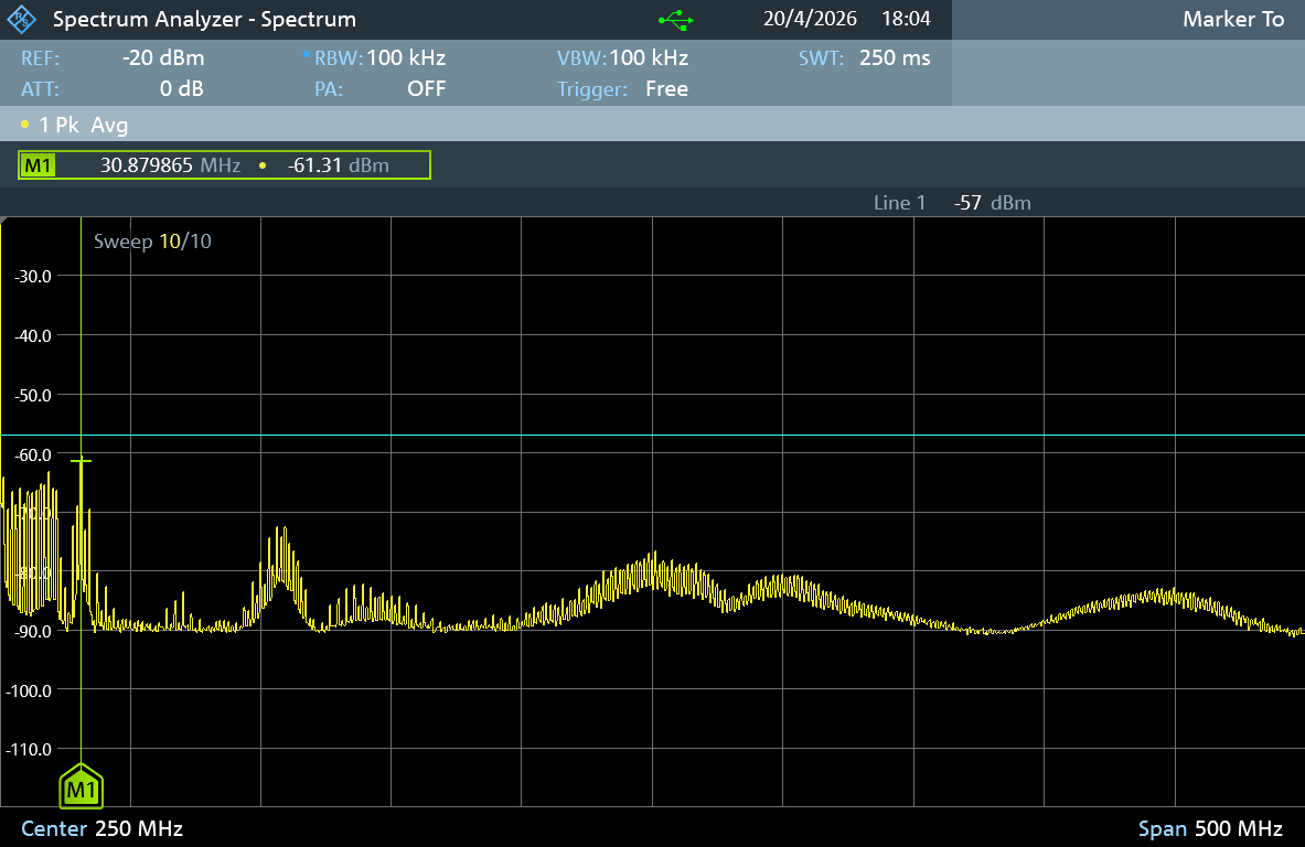
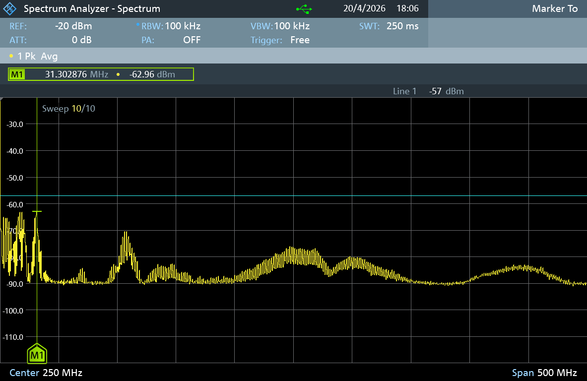
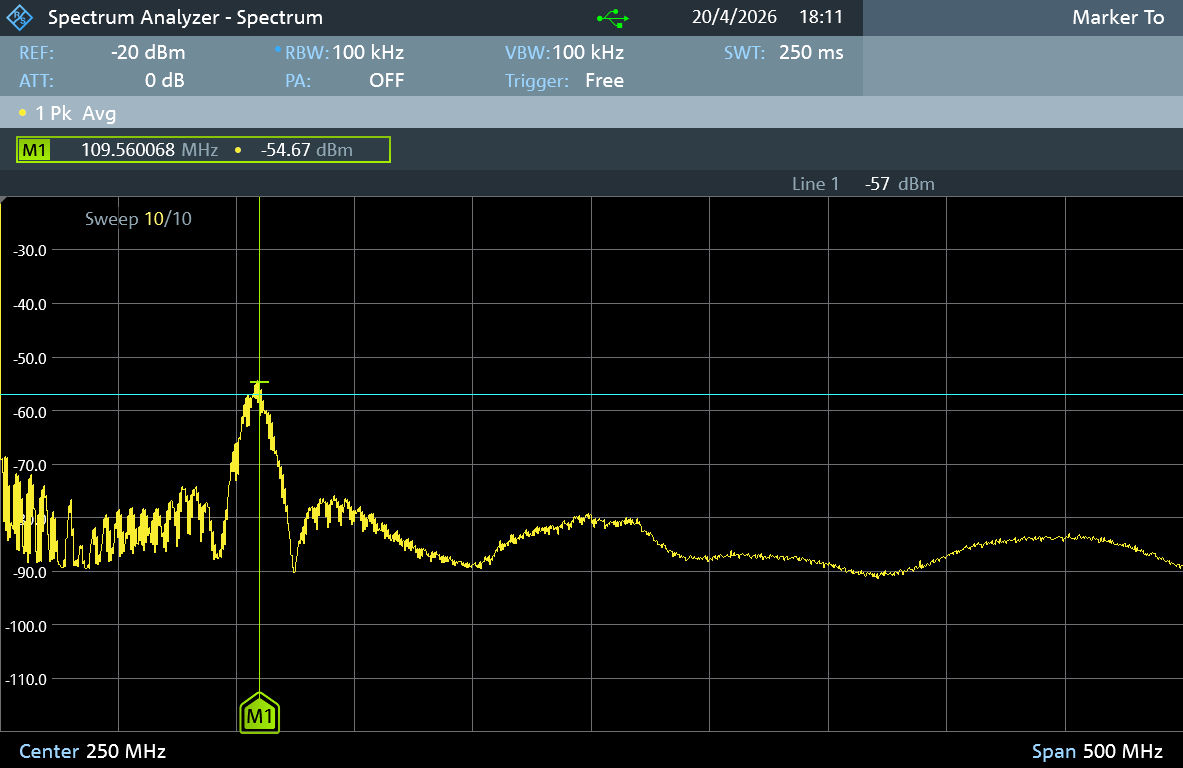
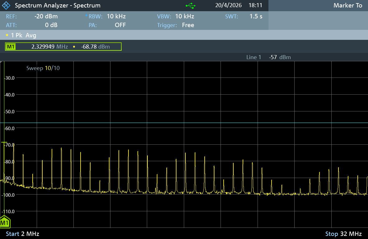
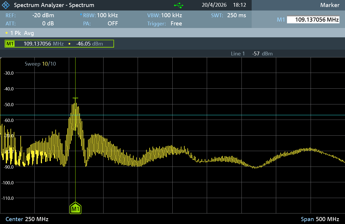
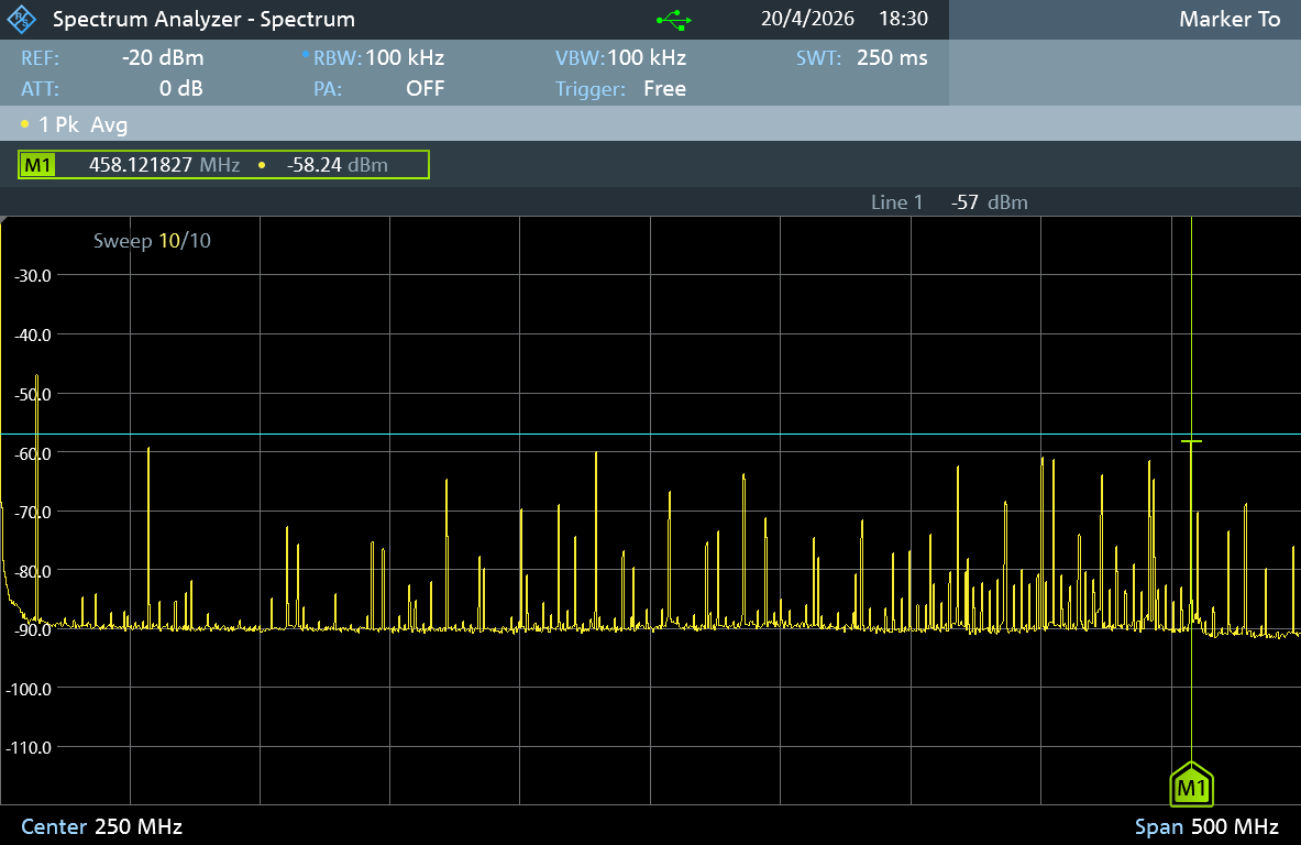
Not wanting my concoction to cause excessive spurious emissions through the KX2's antenna port, I had a look with a spectrum analyzer. I am by no means an expert in this domain, but according to ETSI EN 301 783 clause 5.2.3, the limit for spurious emissions at the antenna port of an amateur radio device in standby mode is -57 dBm in the frequency range of 0.15 to 1000 MHz.
Test conditions
KX2 in off mode (ATU set to bypass before turning off), internal 3S battery charged to around 80%. KX2 antenna port connected directly to spectrum analyzer with 0.5 m LMR 240 cable. Spectrum analyzer set to peak detector mode to capture the worst-case scenario (the standards document is not entirely clear about which detector to use).
Spectrum measurements
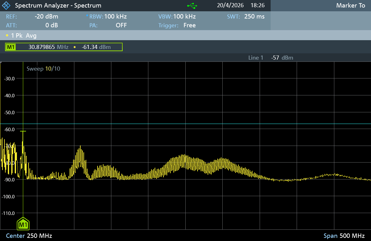
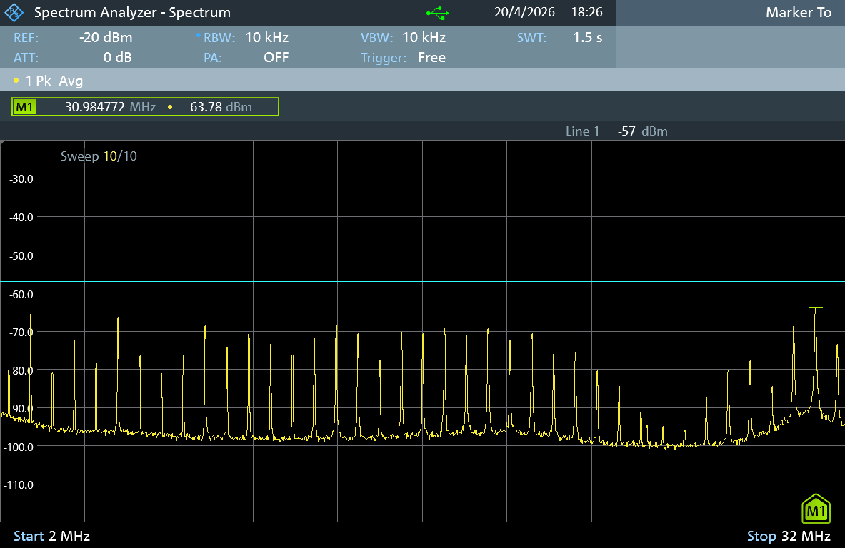
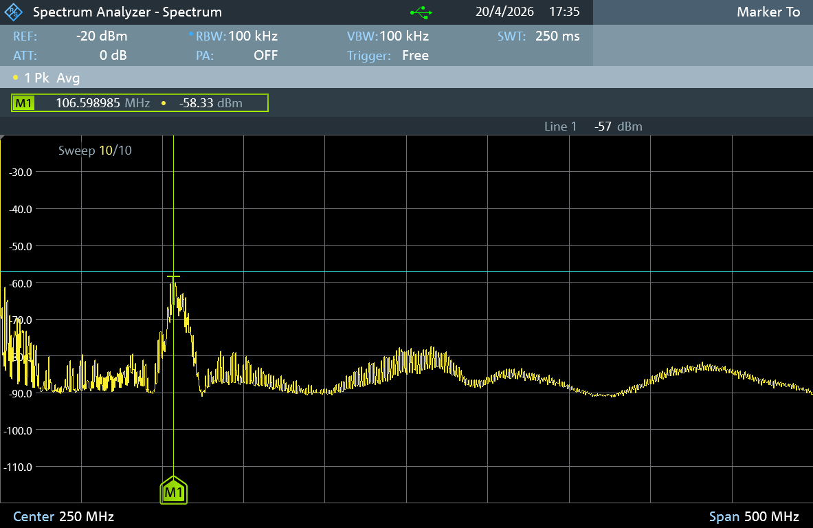
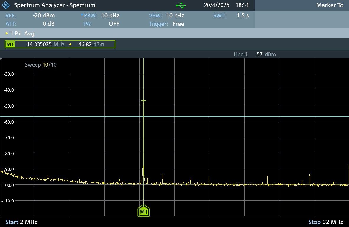
For comparison, here is the spectrum at the antenna port of a KX2 in RX mode (no KXUSBC2 installed) with the pre-amp on and the frequency set to 14.333 MHz:
Summary
When charging at typical power levels (15 V @ 1.6 A was the highest input current encountered during my tests with the maximum battery current set to the default of 2 A), the -57 dBm limit is respected, and also when discharging at typical voltages/currents for an attached smartphone. Only when discharging at both high voltages and high current (12 or 15 V at 2 A) are there spurs around 100 MHz that exceed the limit. It is thus recommended to disconnect the antenna from the KX2 when fast charging external devices. Alternatively, reducing the current to 1.5 A @ 12 V or 1 A @ 15 V also reduces those spurs to below the limit.
Empirical test on summit with EFHW
Finally, to check the situation that interests the SOTA activator the most, I did a quick empirical test on a summit in a typical setup, with a 40/30/20m EFHW connected to the KX2 in SSB mode. Then I tried charging my iPhone at 10 W (9 V) from the KXUSBC2, and in a separate test, charging the KX2's battery from an external power bank at 18 W (12 V) while operating (auto-suspend feature disabled). In both cases, I could not discern a difference in noise floor on 80-20m, despite disconnecting/reconnecting the USB source/sink many times to find out. There were some spurious wandering signals around 14.310 MHz that I could trace to the charger, probably the 9th harmonic mentioned above, which was even higher now because it was cold on the summit.
Needless to say, it is not recommended to transmit while charging (as the PA drawing current from the charger may lead to increased TX noise/spurs), and by default, this situation is not possible anyway.
So to sum it up: QRM doesn't seem to be a big issue, even if you're charging while operating. And when not charging, the switching converter is completely off, so no QRM.